In-DRAM Bulk Bitwise Execution Engine 第二节 Background on DRAM 解读。
Background on DRAM 主要讨论了以下话题:
- 1.1 memory cell 的电气原理
- 1.2 die 的构成
- 1.3 memory controller 与 die 的对接
Figure 1 shows the organization of the memory subsystem in a modern computing system.
-
CPU <-> memory controller <-> memory channels
At a high level, each processor chip is connected to one or more off-chip memory channels.
Each memory channel consists of its own set of command, address, and data buses.
Depending on the design of the processor, there can be either an independent memory controller for each memory channel or a single memory controller for all memory channels.
-
memory channel <-> memory module
All memory modules connected to a channel share the buses of the channel.
-
memory module <-> chip
从物理构造的角度看,module 确实由 device / chip 组成。
从 CPU 访问角度看,CPU 主要访问 logical rank。logical rank 和 device / chip 是正交关系。
section 2 主要讨论 device / chip 的构造(实际上只讨论到 bank 层级,bank group 都没有讨论)。section 3 会谈论 logical rank。
Each memory module consists of many DRAM devices (or chips).
Most of this section is dedicated to describing the design of a modern DRAM chip.
In Section 3, we present more details of the module organization of commodity DRAM.
注意,这节说的 chip 实际上是 die。chip / device 和 die 的关系,和封装有关系,另外进行讨论。
主要介绍 capacitor 能存储电荷,以及 senseamp 基本原理。
-
Capacitor
At the lowest level, DRAM technology uses capacitors to store information.
Specifically, it uses the two extreme states of a capacitor, namely, the empty and the fully charged states to store a single bit of information.
For instance, an empty capacitor can denote a logical value of 0, and a fully charged capacitor can denote a logical value of 1.
Figure 2 shows the two extreme states of a capacitor.
-
Need for sense amplifier
-
Capacitors are small, charges are small, differences between 2 states are small
Unfortunately, the capacitors used for DRAM chips are small, and will get smaller with each new generation.
As a result, the amount of charge that can be stored in the capacitor, and hence the difference between the two states is also very small.
-
Capacitor can lose state
意思大概是说,capacitor 上的电荷会流走。
In addition, the capacitor can potentially lose its state after it is accessed.
-
-
Sense amplifier
Therefore, to extract the state of the capacitor, DRAM manufacturers use a component called sense amplifier.
Figure 3 shows a sense amplifier.
-
Two inverters with enable signal
A sense amplifier contains two inverters which are connected together such that the output of one inverter is connected to the input of the other and vice versa.
The sense amplifier also has an enable signal that determines if the inverters are active.
-
Two stable states
When enabled, the sense amplifier has two stable states, as shown in Figure 4. In both these stable states, each inverter takes a logical value and feeds the other inverter with the negated input.
-
Operation example
Figure 5 shows the operation of the sense amplifier, starting from a disabled state.
In the initial disabled state, we assume that the voltage level of the top terminal (V a ) is higher than that of the bottom terminal (V b ).
When the sense amplifier is enabled in this state, it senses the difference between the two terminals and amplifies the difference until it reaches one of the stable states (hence the name “sense amplifier”).
-
使用 transistor 连接 capacitor 和 senseamp,memory cell 的基本雏形已经出来。
同时加入两个命令 ACTIVATE 和 PRECHARGE,驱动 wordline、senseamp enable、PRECHARGE unit,senseamp 可以读出 capacitor 的状态,放在 bitline 上,或者回到初始状态。
可以看到,这里已经开始引入命令了,但是没有明说命令是谁发的。
-
Convert state of capacitor to state of sense amplifier
DRAM technology uses a simple mechanism that converts the logical state of a capacitor into a logical state of the sense amplifier.
Data can then be accessed from the sense amplifier (since it is in a stable state).
Figure 6 shows 1) the connection between a DRAM cell and the sense amplifier, and 2) the sequence of states involved in capturing the cell state in the sense amplifier.
-
Wordline and bitline connect capacitor and sense amplifer
As shown in the figure (state 1), the capacitor is connected to an access transistor that acts as a switch between the capacitor and the sense amplifier.
The transistor is controller by a wire called wordline.
The wire that connects the transistor to the top end of the sense amplifier is called bitline.
-
1 Precharged state
也叫 idle state。
In the initial state 1,
- the wordline is lowered,
- the sense amplifier is disabled and
- both ends of the sense amplifier are maintained at a voltage level of 1/2 VDD.
We assume that the capacitor is initially fully charged (the operation is similar if the capacitor was initially empty).
This state is referred to as the precharged state.
-
Activated state
An access to the cell is triggered by a command called ACTIVATE.
命令参数:ACT 命令只需要 bank ID 和 row。
语义:打开这个 row。
时序参数:发完 ACT 命令以后,要等 tRCD,让下面这些流程完成。
动作:raise wordline、charge sharing、senseamp enable。
结果:一、row 的数据出现在 senseamp 里(即打开 row)。二、电容里面的电荷和原来一样,要么是满的,要么是空的。
-
2 Wordline high
Upon receiving an ACTIVATE, the corresponding wordline is first raised (state 2). This connects the capacitor to the bitline.
-
3 Charge sharing
In the ensuing phase called charge sharing (state 3), charge flows from the capacitor to the bitline, raising the voltage level on the bitline (top end of the sense amplifier) to 1/2 VDD + δ.
-
4 Enable senseamp and 5 activated state
After charge sharing, the sense amplifier is enabled (state 4).
The sense amplifier detects the difference in voltage levels between its two ends and amplifies the deviation, till it reaches the stable state where the top end is at VDD (state 5).
Since the capacitor is still connected to the bitline, the charge on the capacitor is also fully restored.
-
-
Read or Write
We shortly describe how the data can be accessed from the sense amplifier.
-
Back to precharged state
命令参数:PRECHARGE 命令只需要选择一个 bank。因为一个 bank 只有一排 senseamp,一个时刻只有一条 wordline high,所以不需要选择 row。
语义:关闭 bank 里打开的 row。
时序参数:发完 PRE 命令以后,要等 tRP,让下面这些流程完成。
动作:lower wordline、sensemap 关闭、用 precharge unit 把 senseamp 恢复 1/2 VDD。
结果:一、senseamp 与 row 的连接断开。二、senseamp 电压回到初始值,之前从 row 里读出来的数据丢失(即关闭 bank 里打开的 row),为下一次工作做准备。
However, once the access to the cell is complete, the cell is taken back to the original precharged state using the command called PRECHARGE.
- Upon receiving a PRECHARGE, the wordline is first lowered, thereby disconnecting the cell from the sense amplifier.
- senseamp 关闭
- Then, the two ends of the sense amplifier are driven to 1/2 VDD using a precharge unit (not shown in the figure for brevity).
这三个动作和上面的 precharged state 三个状态相对。
另外,PRECHARGE 实际上是一个很奇怪的名字。谁在给谁充电?实际上,早期 DRAM 确实会给位线充电,灌满电荷到 VDD。但是那种方案有很多问题,所以演化成现在的方案。但是现在的方案里实际上没有充电,只是沿用了以前的名字。
现在的方案里 precharge 电路主要做两件事。
第一件事,是用一个均衡晶体管把 BL 和 BL̄ 直接短接起来。
计算一下(两条位线电容都是 C,做得几乎一样):
- 短接前:高的那条带电荷 Q = C·VDD,低的那条带 0。总电荷 = C·VDD。
- 短接后:两条并起来总电容 2C,电荷守恒还是 C·VDD。
- 所以共同电位 = 总电荷 / 总电容 = C·VDD / 2C = VDD/2。
高位线上的正电荷顺着这根短接管流一半到低位线,两条位线在正中间会合。电荷一点没多、一点没少,只是从一条挪到了另一条。这一步从电源取的电荷是零。所以「充到 VDD/2」更准确说是「平均到 VDD/2」,是重分配,不是充电。
第二件事:接到 VBLP 参考电压做微调。
现实里两条位线电容不完全相等、还有泄漏,光靠短接不一定精确停在 VDD/2。所以 precharge 电路还有两个管子把 BL、BL̄ 连到一个片上生成的 VDD/2 参考电平(VBLP),把绝对值校准并钉住在 VDD/2。这一步会从这个参考源取/吐一点点电荷来纠偏,但量很小,大头已经被上面的电荷共享搞定了。
所以真要较真,PRECHARGE 应该叫 EQUALIZE。
senseamp 和 wordline driver 不可能每个 cell 一个,实际上是多个 cell 共享的。
朴素的 2D array 利用率不够,实际上是 open bitline 架构。
采用 open bitline 架构的 2D cell array 就被叫做 MAT/Tile。
-
DRAM manufacturers want to maximize density
A major goal of DRAM manufacturers is to maximize the density of the DRAM chips while adhering to certain latency constraints (described in Section 2.2.6).
-
Two costly components
There are two costly components in the setup described in the previous section.
-
Sense amplifier
The first component is the sense amplifier itself.
Each sense amplifier is around two orders of magnitude larger than a single DRAM cell [122, 92].
-
Wordline logic
Second, the state of the wordline is a function of the address that is currently being accessed. The logic that is necessary to implement this function (for each cell) is expensive.
-
-
Two costly components are shared
In order to reduce the overall cost of these two components, they are shared by many DRAM cells.
-
Each sense amplifier is shared by a column of cells
Specifically, each sense amplifier is shared by a column of DRAM cells.
In other words, all the cells in a single column are connected to the same bitline.
-
Each wordline is shared by a row of cells
Similarly, each wordline is shared by a row of DRAM cells.
-
-
2D array
Together, this organization consists of a 2-D array of DRAM cells connected to a row of sense amplifiers and a column of wordline drivers.
Figure 7 shows this organization with a 4 × 4 2-D array.
-
Open bitline architecture
2D array 实际上有两排 senseamp,cell 密度翻一倍。
To further reduce the overall cost of the sense amplifiers and the wordline driver, modern DRAM chips use an architecture called the open bitline architecture [31].
-
Two observations
This architecture exploits two observations.
-
Sense amplifier is wider than DRAM cells
First, the sense amplifier is wider than the DRAM cells.
This difference in width results in a white space near each column of cells.
-
Sense amplifier is symmetric
Second, the sense amplifier is symmetric.
Therefore, cells can also be connected to the bottom part of the sense amplifier.
-
-
Example
Putting together these two observations, we can pack twice as many cells in the same area using the open bitline architecture, as shown in Figure 8;
As shown in the figure, a 2-D array of DRAM cells is connected to two rows of sense amplifiers: one on the top and one on the bottom of the array.
While all the cells in a given row share a common wordline, half the cells in each row are connected to the top row of sense amplifiers and the remaining half of the cells are connected to the bottom row of sense amplifiers.
-
-
DRAM MAT/Tile
This tightly packed structure is called a DRAM MAT/Tile [144, 155, 82].
In a modern DRAM chip, each MAT typically is a 512×512 or 1024×1024 array.
Multiple MATs are grouped together to form a larger structure called a DRAM bank, which we describe next.
开始讲 bank 的构造。
逻辑上看,bank 就是一个 MAT/Tile 加上 row decoder、column selection logic、bank IO logic。
实际上,bank 是一个 MAT/Tile 的 2D array。
注意,本节又开始讨论和外界的接口了,并且说明了数据交换的节奏。
-
Bank is the smallest structure visible to mem controller
In most modern commodity DRAM interfaces [65, 66, 83], a DRAM bank is the smallest structure visible to the memory controller.
All commands related to data access are directed to a specific bank.
-
Logical structure of a bank
一个 bank 从逻辑上看,就是一个 2d array。
Logically, each DRAM bank is a large monolithic structure with a 2-D array of DRAM cells connected to a single set of sense amplifiers (also referred to as a row buffer).
For example, in a 2Gb DRAM chip with 8 banks, each bank has 2^15 rows and each logical row has 8192 DRAM cells.
验证一下,8 (2^3) x 2^15 x 8192 (2^13) = 2^31。
Figure 9 shows this logical view of a bank.
In addition to the MAT, the array of sense amplifiers, and the wordline driver, each bank also consists of some peripheral structures to decode DRAM commands and addresses, and manage the inputs/outputs to the DRAM bank.
-
Row decoder
Specifically, each bank has a row decoder to decode the row address associated with row-level commands (e.g., ACTIVATE).
-
Column selection logic
这里说的一个 column,实际上不是一个 cell,而是位宽个 cell(比如 x4、x8、x16)。位宽由 die 决定。
所以 column selection logic 也不用选单个 cell。
Each data access command (READ and WRITE) accesses only a part of a DRAM row.
Such an individual part is referred to as a column.
With each data access command, the address of the column to be accessed is provided.
This address is decoded by the column selection logic.
-
Bank I/O logic
Depending on which column is selected, the corresponding piece of data is communicated between the sense amplifiers and the bank I/O logic.
The bank I/O logic in turn acts as an interface between the DRAM bank and the chip-level I/O logic.
-
-
Logical structure 解析
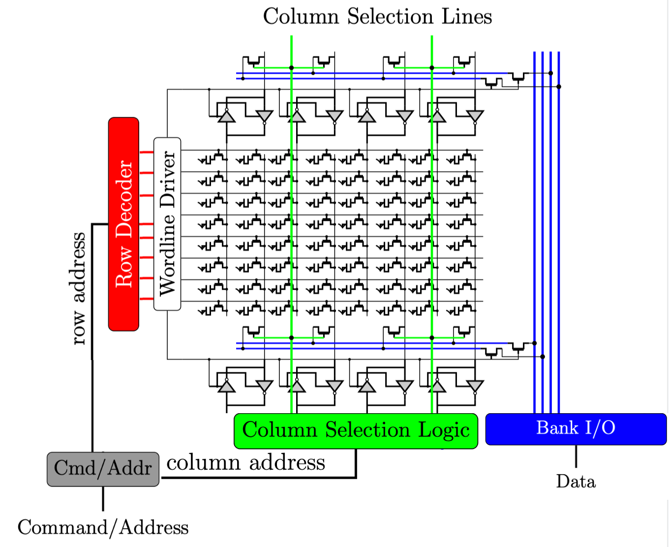
这个图是我自己做的。
假设有一个 x2 2n prefetch bank,有 8 行,每行 8 个 bit。
RA 3 bit,经过 row decoder 选择 8 行中的 1 行。
wordline driver 让这一条 wordline 先升高,电荷共享后,senseamp enable 也升高。经过一段时间,这一行的 8 个 bit 都进入了 senseamp。
一个 column 2 bit(x2),一次读写命令访问 2 个 column(2n prefetch)。8 bit 总共有 2 个 2n。
所以 CA(0) 不驱动 CSL,CA(1) 驱动 CSL 来选 2 个 2n 中的一个,CSL 实际上也是一个 decoder。选好了以后,一共 4 bit 放进 bank I/O。
-
Physical structure of a bank
-
Building a large MAT is not feasible
前面说了,一个 MAT 一般只有 512x512 或者 1024x1024,再大不太可能。
Although the bank can logically be viewed as a single MAT, building a single MAT of a very large size is practically not feasible as it would require very long bitlines and wordlines (leading to very high latencies).
-
Bank is 2-D array of MATs
Therefore, each bank is physically implemented as a 2-D array of DRAM MATs.
Figure 10 shows a physical implementation of the DRAM bank with 4 MATs arranged in a 2 × 2 array.
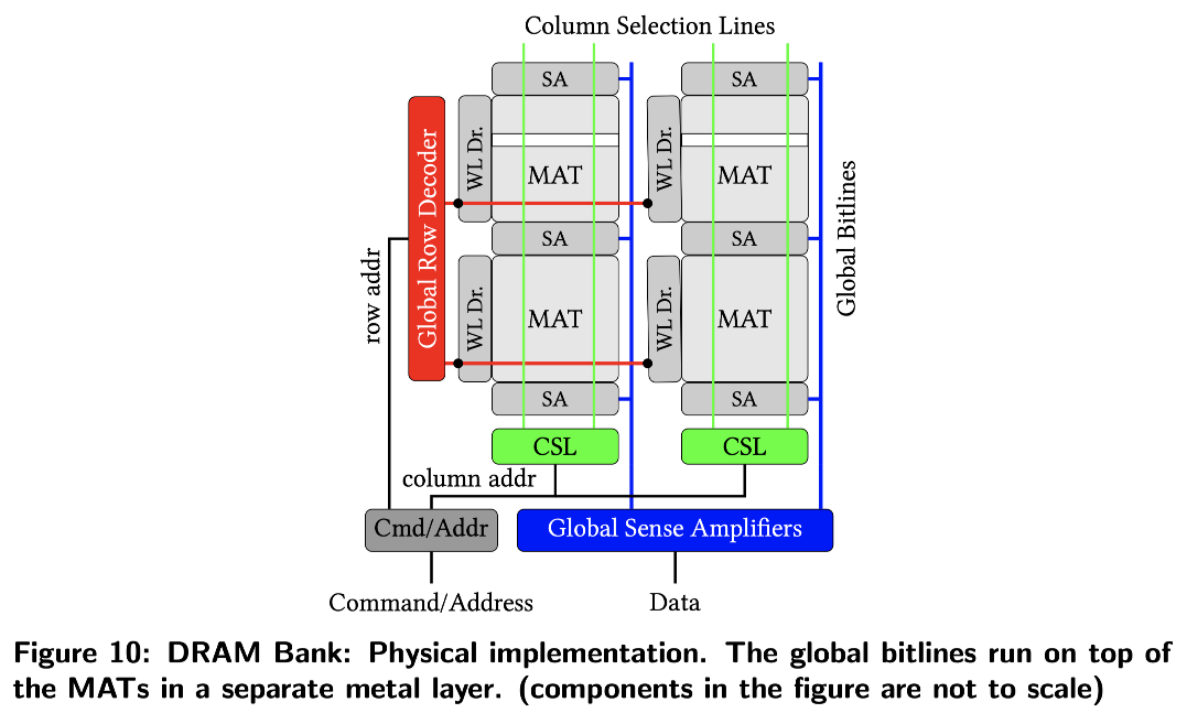
这个图我加了两条绿线。
-
Global row decoder
row 说法有点问题,具体看下面讨论。
As shown in the figure, the output of the global row decoder is sent to each row of MATs.
-
Global senseamp and global bitline
这说法倒是没什么问题。
The bank I/O logic, also known as the global sense amplifiers, are connected to all the MATs through a set of global bitlines.
As shown in the figure, each vertical collection of MATs has its own column selection logic (CSL) and global bitlines.
In a real DRAM chip, the global bitlines run on top of the MATs in a separate metal layer.
Data of each column is split equally across a single row of MATs. With this data organization, each global bitline needs to be connected only to bitlines within one MAT.
While prior work [144] has explored routing mechanisms to connect each global bitline to all MATs, such a design incurs high complexity and overhead.
-
-
Physical structure of a MAT in a bank
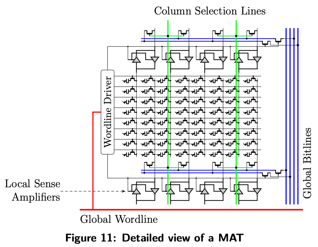
这个图是原图。row 依旧有问题,column 没啥问题。
Figure 11 shows the zoomed-in version of a DRAM MAT with the surrounding peripheral logic.
Specifically, the figure shows how each column selection logic selects specific sense amplifiers from a MAT and connects them to the global bitlines.
We note that the width of the global bitlines for each MAT (typically 8/16) is much smaller than that of the width of the MAT (typically 512/1024).
This is because the global bitlines span a much longer distance across the chip and hence have to be wider to ensure signal integrity.
-
-
Physical structure 解析
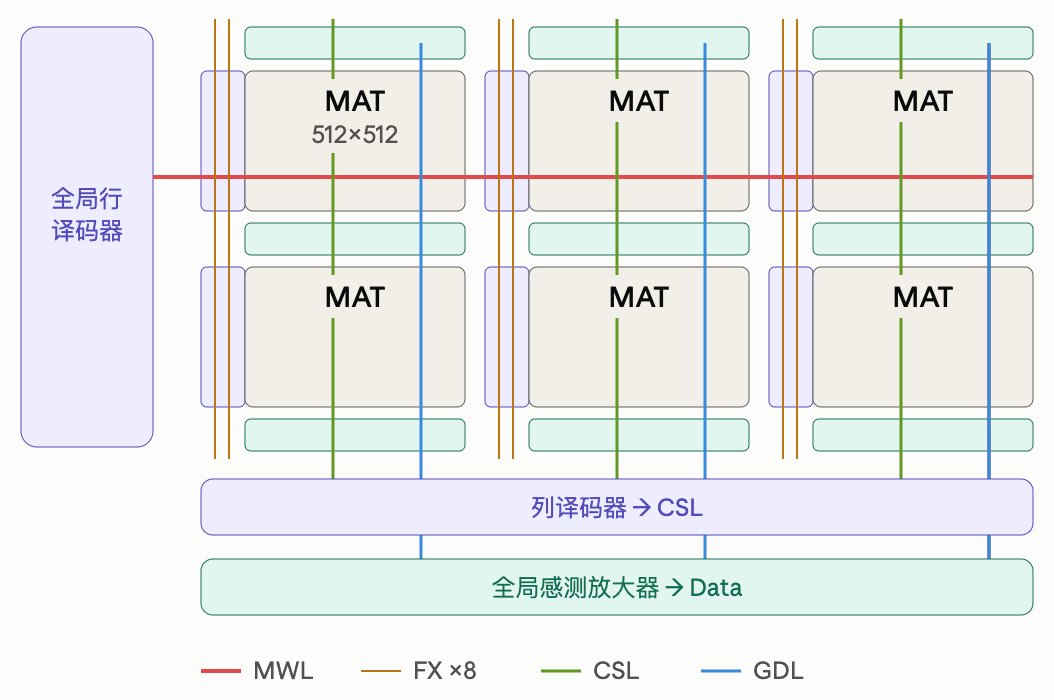
一个 bank 实际上是 MAT/Tile 的 2D array。MAT/Tile 一般是 512x512 或者 1024x1024。
对于一个 8Gb x8 的 die,16 个 bank,column 10 根线,row 16 根线。那么一个 bank 的逻辑结构是,2^16 个 row,2^10 个 column,一个 column 8 个 bit。
如果我们选用 512x512 的 MAT/Tile,那么我们需要 128 行 16 列 MAT/Tile。
首先关注 row。
全局行译码器 global row decoder 的输入是 RA(15:3),输出是 8192 根 MWL(main wordline)。
FX 译码器的输入是 RA(2:0),输出 8 根 FX。RA 的低三位给 FX 是常见配置,跟 die 的容量无关。
紫色竖直长条是 wordline driver,一个 MAT 的 wordline driver 输入 64 根 MWL 和 8 根 FX,输出 512 根 SWL(sub wordline)。64 乘 8 正好等于 512。举个具体例子,对于第一行 MAT,RA(15:3) 都为 0 对应上面 8 行,然后再根据 FX 选择这 8 行中对应的 1 行,驱动 SWL。
再看 column。
因为 8n prefetch,所以 CA(2:0) 不进列译码器。列译码器输入 CA(9:3),输出 128 根 CSL(Column Selection Line)。注意,每一列 MAT 都有相同的 128 根 CSL。1 根 CSL 亮起来以后,16 列 MAT 里面位置编号相同的 4 个 senseamp 的 4 bit 会拼成 64 bit。
所以数据的位置实际上很乱,不存在 8 个连续的 bit 构成一个字节。
数据的路径:sense amp → LDL(MAT 内部的短数据线)→ GDL(图上的蓝线,跨 MAT 的长线)→ 底下的全局感测放大器 → Data。
-
DRAM chip has multiple banks
层次有点问题,这里说的 chip 对内指 die 的 bank group,对外指 die。
Each DRAM chip consists of multiple banks, as shown in Figure 12.
All the banks share the chip’s internal command, address, and data buses.
As mentioned before, each bank operates mostly independently (except for operations that involve the shared buses).
-
Data transfer between chip and bank
这里说的 chip 对外,指 die。
The chip I/O logic manages the transfer of data to and from the chip’s internal bus to the memory channel.
-
Width of chip output n and width of bank output 8n
chip output 宽度就是 n,bank output 宽度是 8n。
The width of the chip output (typically 8 bits) is much smaller than the output width of each bank (typically 64 bits).
-
Bank output 8n is buffered at chip IO and sent out n/half cycle
bank output 被缓存在 chip IO,然后 chip 半个周期发出 n 个 bit。
Any piece of data accessed from a DRAM bank is first buffered at the chip I/O and sent out on the memory bus 8 bits at a time.
With the DDR (double data rate) technology, 8 bits are sent out each half cycle.
-
4 cycles to sent out 8n
Therefore, it takes 4 cycles to transfer 64 bits of data from a DRAM chip I/O logic on to the memory channel.
-
专门讲命令。
这里的 chip 主要指 bank group。
-
Data access requires bank ID, row, column
To access a piece of data from a DRAM chip, the memory controller must first identify the location of the data: the bank ID (B), the row address (R) within the bank, and the column address (C) within the row.
After identifying these pieces of information, accessing the data involves three steps.
-
PRECHARGE with bank ID
命令参数:PRECHARGE 命令只需要选择一个 bank。因为一个 bank 只有一排 senseamp,一个时刻只有一条 wordline high,所以不需要选择 row。
语义:关闭 bank 里打开的 row。
时序参数:发完 PRE 命令以后,要等 tRP,让下面这些流程完成。
动作:lower wordline、sensemap 关闭、用 precharge unit 把 senseamp 恢复 1/2 VDD。
结果:一、senseamp 与 row 的连接断开。二、senseamp 电压回到初始值,之前从 row 里读出来的数据丢失(即关闭 bank 里打开的 row),为下一次工作做准备。
The first step is to issue a PRECHARGE to the bank B.
This step prepares the bank for a data access by ensuring that all the sense amplifiers are in the precharged state (Figure 6, state 1).
No wordline within the bank is raised in this state.
-
ACTIVATE with bank ID and row
命令参数:ACT 命令只需要 bank ID 和 row。
语义:打开这个 row。
时序参数:发完 ACT 命令以后,要等 tRCD,让下面这些流程完成。
动作:raise wordline、charge sharing、senseamp enable。
结果:一、row 的数据出现在 senseamp 里(即打开 row)。二、电容里面的电荷和原来一样,要么是满的,要么是空的。
The second step is to activate the row R that contains the data.
This step is triggered by issuing an ACTIVATE to bank B with row address R.
Upon receiving this command, the corresponding bank feeds its global row decoder with the input R.
The global row decoder logic then raises the wordline of the DRAM row corresponding to address R and enables the sense amplifiers connected to that row.
This triggers the DRAM cell operation described in Section 2.2.2.
At the end of the activate operation, the data from the entire row of DRAM cells is copied to the corresponding array of sense amplifiers.
-
READ/WRITE with bank ID and column
The third and final step is to access the data from the required column.
This is done by issuing a READ or WRITE command to the bank with the column address C.
Upon receiving a READ or WRITE command, the corresponding address is fed to the column selection logic. The column selection logic then raises the column selection lines (Figure 11) corresponding to address C, thereby connecting those local sense amplifiers to the global sense amplifiers through the global bitlines.
For a read access, the global sense amplifiers sense the data from the MAT’s local sense amplifiers and transfer that data to the chip’s internal bus.
For a write access, the global sense amplifiers read the data from the chip’s internal bus and force the MAT’s local sense amplifiers to the appropriate state.
注意,到目前为止都在讲怎么把数据读出来。如何写入数据呢?我们对着 dram 真实构造讲一下。还是用上面的示意图。
WRITE 之前也必须要 ACTIVATE。
底下那个「全局感测放大器」块在写的时候换了身份:读的时候它是放大器,写的时候这个位置是 write driver,负责把数据推上 GDL。实际电路里读写通路是分开的两套,图上合并画了。
GDL 往上走到各个 MAT 列,经过 MAT 行选开关下到 LDL。这一级挡住了其他 127 个 MAT 行,所以数据只进被激活的那一行。
CA(9:3) 驱动绿色 CSL,打开选中位置的传输门,LDL 接上 sense amp。
关键动作:write driver 的驱动能力被设计得远强于 sense amp 的锁存器,硬把 latch 掀翻。比如原来锁的是 1(BL=VDD,BLB=0),要写 0,driver 就把 BL 强拉低、BLB 强拉高,latch 翻转。
wordline 全程没关过。latch 一翻,电容里的电荷就流进或流出,跟到新值。
-
-
Not all data accesses require all three steps
Not all data accesses require all three steps.
-
Row buffer hit
Specifically, if the row that is to be accessed is already activated in the corresponding bank, then the first two steps can be skipped and the data can be directly accessed by issuing a READ or WRITE to the bank.
For this reason, the array of sense amplifiers are also referred to as a row buffer, and such an access that skips the first two steps is called a row buffer hit.
-
Row buffer miss
Similarly, if the bank is already in the precharged state, then the first step can be skipped. Such an access is referred to as a row buffer miss.
-
Row buffer conflict
Finally, if a different row is activated within the bank, then all three steps have to be performed. Such an access is referred to as a row buffer conflict.
-
-
Different operations different time
Different operations within DRAM consume different amounts of time.
-
Memory controller must wait between commands
Therefore, after issuing a command, the memory controller must wait for a sufficient amount of time before it can issue the next command.
-
Timing constraints
Such wait times are managed by pre-specified fixed delays, called the timing constraints.
Timing constraints essentially dictate the minimum amount of time between two commands issued to the same bank/rank/channel.
Table 1 describes some key timing constraints along with their values for the DDR3-1600 interface.
tRAS ACTIVATE → PRECHARGE Time taken to complete a row activation operation in a bank tRCD ACTIVATE → READ/WRITE Time between an activate command and a column command to a bank tRP PRECHARGE → ACTIVATE Time taken to complete precharge operation in a bank tWR WRITE → PRECHARGE Time taken to ensure that data is safely written to the DRAM cells after a write operation (called write recovery) -
Reason for timing constraints
The reason as to why these constraints exist is discussed in prior works [82, 92, 32, 62].
-
Modules <-> rank <-> DRAM chips
-
READ/WRITE for a chip involves 8n bits
As mentioned before, each READ or WRITE command for a single DRAM chip typically involves only 64 bits.
-
Rank
In order to achieve high memory bandwidth, commodity DRAM modules group several DRAM chips (typically 4 or 8) together to form a rank of DRAM chips.
-
Chips in a rank share command/address bus, but have independent data bus
The idea is to connect all chips of a single rank to the same command and address buses, while providing each chip with an independent data bus.
In effect, all the chips within a rank receive the same command with the same address, making the rank a logically large DRAM chip.
Figure 13 shows the logical organization of a DRAM rank.
-
READ/WRITE for a rank involves 64 bytes
Many commodity DRAM ranks consist of 8 chips with each chip accessing 8 bytes of data in response to each READ or WRITE command.
Therefore, in total, each READ or WRITE command accesses 64 bytes of data, the typical cache line size in many processors.
-